TSMC Targets 12-Inch Silicon Carbide as Key Thermal Material for the AI Era
The global semiconductor industry is entering a new era driven by artificial intelligence (AI) and high-performance computing (HPC), where thermal management has become the critical bottleneck in chip design and manufacturing. As advanced packaging technologies such as 3D stacking and 2.5D integration push chip density and power consumption to new limits, traditional ceramic substrates can no longer keep up with rising thermal flux requirements.
In response, foundry leader TSMC is making a bold materials shift—embracing 12-inch silicon carbide (SiC) single-crystal substrates while gradually phasing out its gallium nitride (GaN) business by 2027. This recalibration underscores that thermal management is no longer a “supporting technology,” but a core competitive advantage in the AI and HPC era.
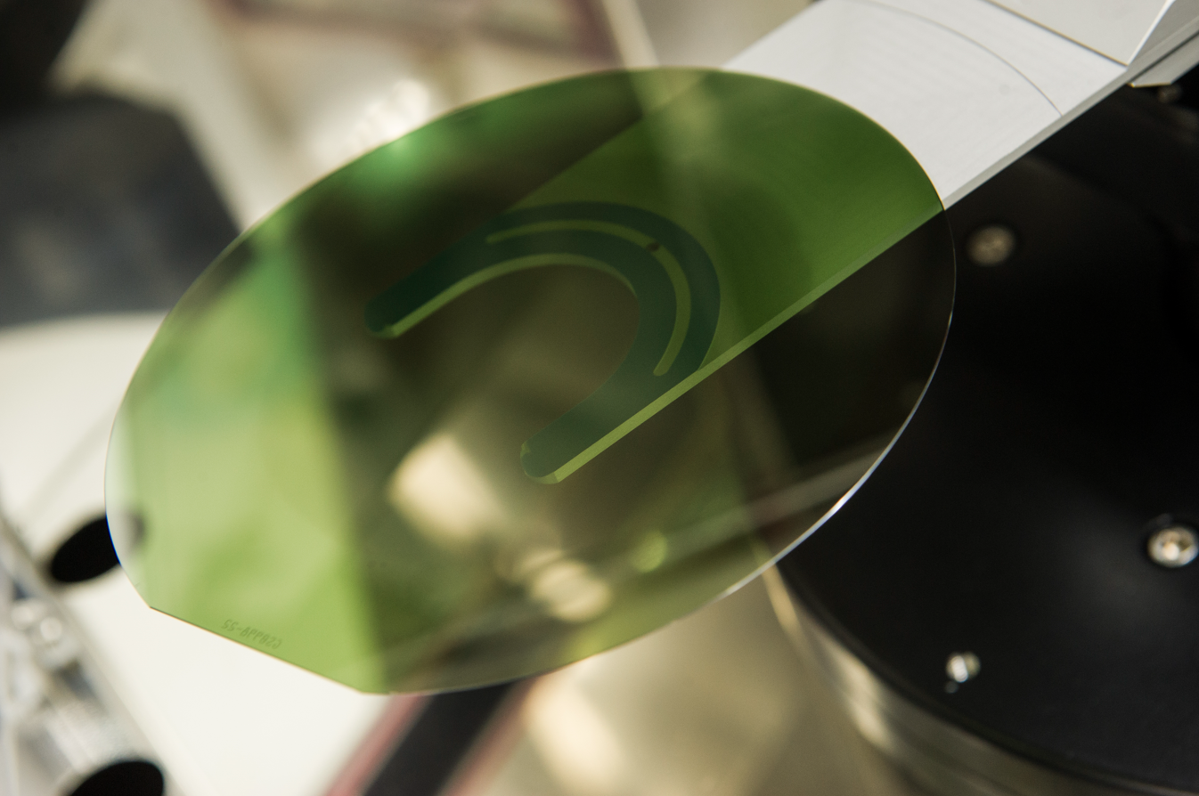
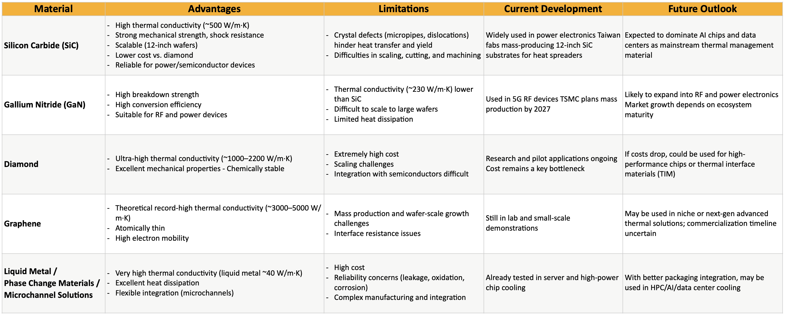
SiC, traditionally used in EV inverters and power electronics, brings significant advantages for thermal applications, with thermal conductivity of around 500 W/mK—far higher than alumina or sapphire substrates. This makes SiC particularly attractive for AI accelerators, data center processors, and wearable devices, where limited space and rising power densities make heat dissipation increasingly critical.
Unlike power devices, thermal management applications do not require the strictest standards for electrical defects, but crystal integrity and mechanical stability remain essential. Warpage, deformation, and surface flatness directly affect chip alignment and advanced packaging yields, especially at the 12-inch scale. Industry priorities are shifting toward uniform density, low porosity, and high flatness as prerequisites for high-yield SiC thermal substrates.
SiC also offers unique benefits for advanced packaging. In 2.5D integration, heat challenges are primarily horizontal, while in 3D stacking, vertical interconnects drastically increase thermal stress. SiC can act as a passive heat spreader or be integrated with diamond, liquid metal, or other advanced cooling technologies in hybrid systems. While materials like diamond and graphene offer higher conductivity, their costs and scalability remain prohibitive. SiC strikes the best balance of performance, strength, and manufacturability, making it the most practical solution for mass deployment.
Leveraging its deep expertise in 12-inch wafer processing, TSMC can accelerate the integration of SiC into existing production lines without rebuilding its manufacturing ecosystem, ensuring both cost and yield advantages. This positions TSMC ahead of competitors in translating material innovation into system-level thermal solutions.
TSMC’s decision to redirect resources from GaN to SiC reflects a long-term strategy: while GaN has strengths in high-frequency devices, SiC provides broader scalability and superior thermal management. The transition to 12-inch SiC wafers reduces unit cost and improves process uniformity, further enhancing competitiveness.
Beyond power electronics, TSMC is pioneering new SiC applications. Conductive N-type SiC can be used as a thermal substrate for AI accelerators and high-performance processors, while semi-insulating SiC interposers can enable chiplet architectures that balance electrical isolation with thermal conduction. These directions signal that SiC is evolving into the thermal backbone of next-generation AI and data center chips.
As rivals like Intel push backside power delivery and co-design approaches, TSMC’s SiC initiative shows that thermal management is no longer secondary—it is becoming the strategic foundation of leadership in the AI era.